The AMD Navi 31 GPU is a small die design with one GCD (Display Compute Die) and six Memory Cache Dies (MCDs). Each external chip houses dual 32-bit memory controllers combined with a large L3 high-speed cache. These less critical memory and block fetch controllers are placed on the cheaper TSMC 6nm process, while the central display chips use TSMC’s 5nm process.
AMD has confirmed that the full Navi 31 GPU has 96MB of L3 (aka Infinity Cache), but the company has yet to confirm L0, L1 and L2 memory. These are mentioned in the new material:
L0 – 3MB – 240% more
L1 – 3MB – 300% more
L2 – 6MB – 50% more
L3 (Infinity Cache) – 96MB (32MB smaller than Navi 21)
The image shows the AMD Navi 31 six Shader Engine layouts, each with 8 dual compute units. AMD doubled the compute throughput by adding dual-issue SIMD to its design but not the core count. That’s why the processor count is 6144, but the effective single-precision computation performance has increased to 61 TFLOPS.
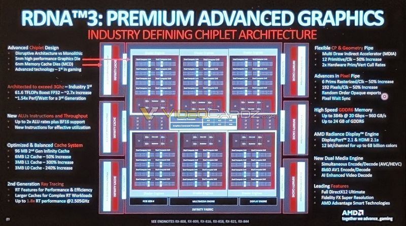
The data also mentions that the RDNA3 architecture will exceed 3GHz. This likely corroborate reports that the architecture is designed to 3.0GHz, although the actual design does not exceed 2.5GHz. The AMD Radeon RX 7900 series is scheduled to launch on December 13. We’re not sure if there’s a separate ban on rDNA3 architectural details, but it’s clear there’s more material that may be seen sooner.
If this article is helpful for you, please share this article with your friends on social media. Thank you!!
Title: Block diagram allegedly leaked for AMD Navi 31 GPU